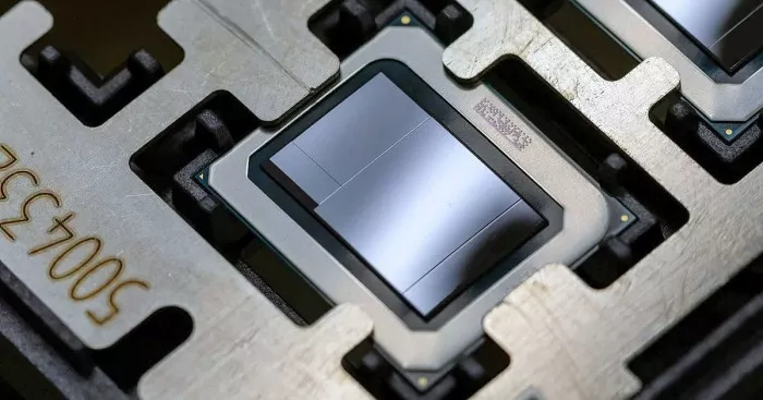
According to the reports in the past period, TSMC has made good progress in the development of 3nm and 2nm processes. Previously, Wei Zhejia, President of TSMC, confirmed that the N2 process node will use gate all around FETs (gaafet) transistors as expected, and the manufacturing process still depends on extreme ultraviolet (EUV) lithography technology. It is expected to make preparations for risk production by the end of 2024 and enter mass production by the end of 2025.

With the breakthrough in the development of 2nm process, TSMC has begun to consider promoting the next process node. It is rumored that the 1.4nm technology may be officially announced at the technical seminar held in June, and some technical details may be announced at that time. According to business Korea, TSMC plans to reassign its N3 process node team in June to form a 1.4nm manufacturing process R & D team.
It is not clear which process Intel and Samsung will adopt to benchmark with TSMC's 1.4nm process. According to the technical roadmap of manufacturing process released by Intel last year, it is currently only arranged to Intel 18a (1.8nm level). Intel plans to introduce two breakthrough technologies, ribbonfet and powervia, into the Intel 20A process node. Recently, it also vowed to launch the improved Intel 18a (1.8nm level) of ribbonfet at the end of 2024, ahead of TSMC's 2nm process, so as to achieve the leading performance per watt.
Many people in the industry are skeptical about the manufacturing process plan of the wafer foundry and worry that more unpredictable obstacles will be encountered in R & D, resulting in delayed mass production time or unsatisfactory yield. As the size of the chip becomes smaller and smaller, the barrier of process technology becomes higher and higher. The circuit must be drawn more accurately. At the same time, it becomes more and more difficult in production management.