Japanese researchers have developed a nano cellulose paper semiconductor, which shows the nano micron macro cross scale designability of 3D structure and the wide adjustability of electrical properties. The research results were recently published in ACS Nano, the core journal of the American Chemical Society. Semiconductor nanomaterials with 3D network structure have high surface area and a large number of pores, which makes them very suitable for applications involving adsorption, separation and sensing.

However, it is still challenging to control electrical properties, create useful micro and macro structures, and achieve excellent functional and end use versatility at the same time.
Cellulose is a natural and easily accessible material derived from wood. Cellulose nanofibers (nano cellulose) can be made into flexible nano cellulose paper (nano paper) sheets with a size similar to that of standard A4 paper. Nanopaper is not conductive, but heating can introduce conductive properties. However, this heat can also damage nanostructures.
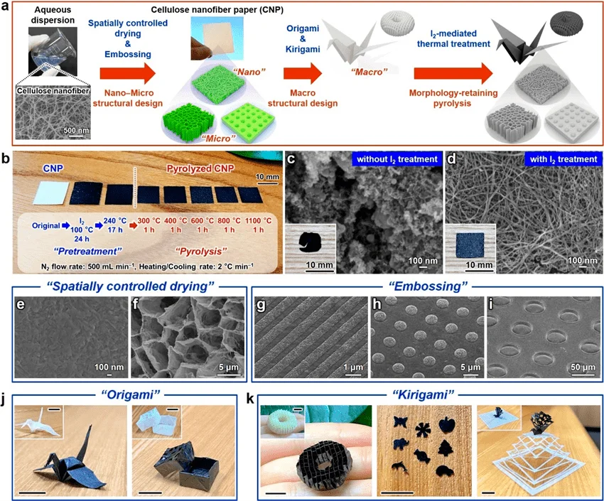
Osaka University researchers, in cooperation with the University of Tokyo, Kyushu University and Okayama University, have designed a treatment process to enable nano paper to be heated without damaging the paper structure from nano scale to macro scale.

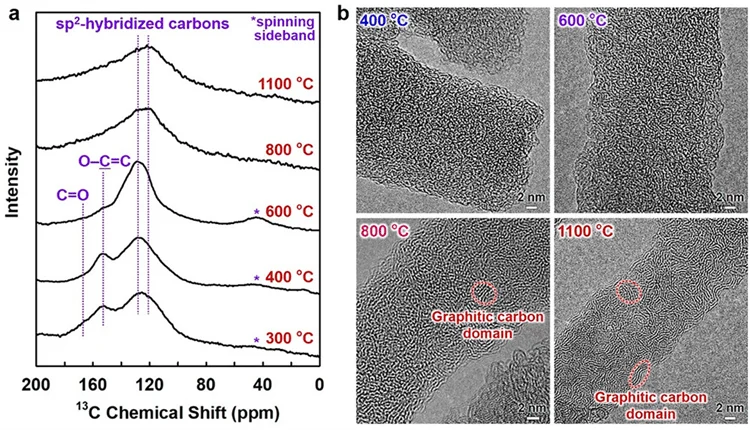
"An important feature of nanopaper semiconductors is tunability because it allows design for specific applications." Associate professor guhebolong, the author of the study, explained that iodine treatment is very effective in protecting the nanostructure of nanopaper. Its combination with spatially controlled drying means that the pyrolysis treatment does not significantly change the structure of the design, and the electrical properties can be controlled using the selected temperature.
Researchers used origami and paper cutting techniques to provide nano paper flexibility at the macro level. They folded the bird and the box and punched out apples And snowflakes, and produce more complex structures by laser cutting. This proves the level of detail that the new process may achieve and that the heat treatment does not cause damage.

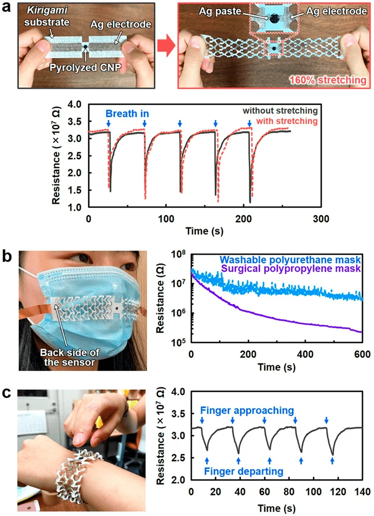
An example of successful application is the combination of nano paper semiconductor sensors into wearable devices to detect moisture exhaled through masks and moisture on skin. Nanopaper semiconductors are also used as electrodes in glucose biofuel cells, generating energy that lights up a small bulb.
Guhebolong said that the structural maintenance and adjustability of the new research to convert nano materials into practical equipment are very encouraging, and the new method lays the foundation for the next development of sustainable electronic products made entirely of plant materials.
