Recently, there have been negative news about Samsung's new process. Previously, there were rumors that the yield was only 35%, which scared away customers such as NVIDIA and Qualcomm. However, Samsung has always denied. Now there are reports that 3nm process has been mass produced, and the most critical yield is also improving. The good news was reported by Samsung's management to the board of directors, which showed Samsung's confidence in the 3nm process and said that the yield has improved, but no specific details have been leaked.
Previously, Samsung announced the Q1 financial report meeting in 2022, and Samsung officials also denied the rumor that the yield rate was not good.
Samsung said that 5nm process has entered a mature stage and is still expanding services. Although the yield improvement process of 4nm process has been delayed, it has entered the predetermined yield curve, and the future 3nm process is still preparing to set up a new R & D production line**

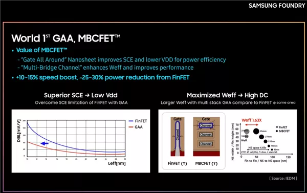
For Samsung, 3nm node is the key for them to bet that the chip process will catch up with TSMC, because TSMC's 3nm process will not be the next generation of GAA transistor technology. Samsung's 3nm node will enable GAA technology, which is a new type of surround gate transistor. Mbcfet (multi bridge channel fet) is manufactured by using nano chip equipment, which can significantly enhance the performance of transistors, It mainly replaces FinFET transistor technology.
According to Samsung, compared with 7Nm manufacturing process, the logical area efficiency of 3nm GAA technology is improved by more than 45%, the power consumption is reduced by 50%, and the performance is improved by about 35%. In terms of paper parameters, it is better than TSMC 3nm FinFET process**